EN
DE

Stories – Trends & Technologies

Trends & Technologies – Expert view

X-ray 4.0: Analyzing nanostructures in real time.

Watch the video 
graphic
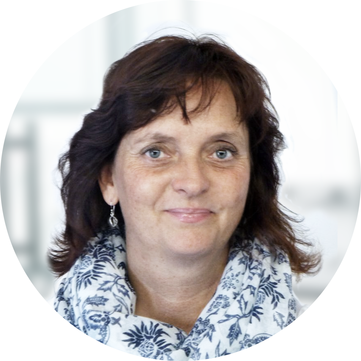
About Antonia Neels

Antonia Neels is Head of the Center for X-Ray Analytics at the Swiss Federal Laboratories for Materials Science and Technology (Empa) and Titular Professor at the University of Fribourg. She grew up in the former East Germany, where she graduated from university with top marks in chemistry shortly after the fall of the Wall. At school, she had chosen French as her second foreign language after Russian. A lucky choice, as otherwise, she would hardly have accepted the doctoral position in x-ray crystallography at the University of Neuchâtel in 1991. Since then, Antonia Neels has been living in Switzerland – now with her husband and two grown-up sons.

As Head of the Center for X-Ray Analytics at Empa, the Swiss Federal Laboratories for Materials Science and Technology, Antonia Neels is developing new methods of x-ray analysis. The focus is on imaging techniques for dynamic processes in the nanometer range. These are particularly groundbreaking for the life sciences, where they facilitate a greater understanding of the interactions between materials and humans.

If Antonia Neels had to pick one item that has shaped her professional career, it would be a crystal. “Crystals don’t just look beautiful, they can also tell us a lot,” she says. Since her research as a PhD student at the University of Neuchâtel more than 30 years ago, she has been involved in x-ray crystallography, a technique for the three-dimensional structural analysis of crystals, crystalline structures (such as silicon) and other types of molecules.

Today, Antonia Neels is head of the Center for X-Ray Analytics at the Swiss Federal Laboratories for Materials Science and Technology (Empa), and she is still fascinated by the “inner workings” of materials. “Curiosity doesn’t get old,” she says. Fortunately, one might add. That’s because the applied research that Neels and 17 other scientists are doing at the Center for X-Ray Analytics is more important than ever for helping to tackle big issues of the future. In effect, x-ray analysis provides the necessary materials knowledge to develop technologies and materials that can make life healthier, safer, more convenient and sustainable.

More effective medicines for an aging society? More efficient batteries for electromobility? More sustainable building materials for CO2 reduction? Smaller microchips for a more digital world? All of this requires a sound knowledge of the molecular structure of materials. “X-ray diffraction and scattering combined with three-dimensional x-ray imaging are ideal for studying materials for their behavior (such as their ductility) and potential defects and then improving them,” says Antonia Neels. “Today, x-ray analysis is one of the most important methodological basis for the development of new materials.”

“Today, x-ray analysis is one of the most important methodological bases for the development of new materials.”

It all comes down to methodology

The further development of these foundational methodologies is the central focus of Empa’s Center for X-Ray Analytics. Here at the Center, combining different x-ray techniques has helped Empa’s research team and numerous industrial partners to analyse ever smaller structures and even observe dynamic processes in real time. In addition to a great deal of know-how, technological progress is also key: more precise detectors, more powerful x-ray equipment, faster processors, better software for data analysis. “Thirty years ago, I wouldn’t have dreamed that we would someday be able to see and analyze molecular interactions in real time,” Antonia Neels marvels. During her time as a doctoral student, it would take her up to five days to complete one crystal structure analysis. This is another reason why Neels soon became interested not only in crystals and other materials, but also in the methodology for studying them.

It was this interest that in 2008 led the native of Berlin, Germany, to the Centre Suisse d’Electronique et de Microtechnique (CSEM) in Neuchâtel – a defining career move away from basic academic research and toward applied materials research. Under Professor Alex Dommann, she set up an x-ray laboratory at CSEM to non-destructively examine and test defects and stresses in semiconductor materials and devices – for example, in pressure sensors. In 2014, with a similar mission, she took over as head of Empa’s Center for X-Ray Analytics. With scientists from various disciplines, she developed a lab that combines methods of x-ray diffraction and scattering with high-resolution imaging techniques, making it unique in Europe today.

Humans and materials

Especially for the semiconductor industry, where non-destructive methods of investigating crystal structures like silicon are crucial, this combination of techniques makes sense. “Crystallography for evaluating strains and defects in combination with morphology, i.e., with the visualization of possible voids and cracks, holds great potential for a better understanding of the processes in semiconductor materials and devices,” says Antonia Neels.

A core interest of the Center for X-ray Analytics is related to the life sciences, a field where it continually explores the interface between humans and materials. For example, when active pharmaceutical compounds encounter human cells, this results in molecular reactions, or biodynamic processes. In clinical trials, investigators want to understand how and where exactly an active ingredient works. And it is precisely here – in the observation of dynamic processes on the nanometer scale and in real time – that modern x-ray analysis develops its full potential.