Stories – Trends
Trends – How Comet is solving for what’s next
First inspection workflow for the semiconductor industry.
Out of the collaboration of the X-Ray Systems team in Hamburg and the recently acquired software developer Object Research Systems (ORS) in Montreal has come a potentially game-changing new offering: VoidInspect, the first x-ray inspection workflow for the semiconductor and electronics market, was developed in 2021 and successfully completed its first customer deployment.
“Last year, we expressed our excitement about the possibility of further leveraging x-ray data to improve our customers’ manufacturing processes,” says Peter Koch, Product Manager, semiconductor/electronics market expert and VoidInspect project lead. “Together with our colleagues in Montreal, we truly brought our vision to life."

“We can analyze images up to 80% faster and make the operation available to any user in only three steps.”
Peter Koch
Product Manager, semiconductor/ electronics market expert and VoidInspect project lead, Hamburg, Germany
X-ray data analysis to reduce waste and drive 80% gain in inspection speed
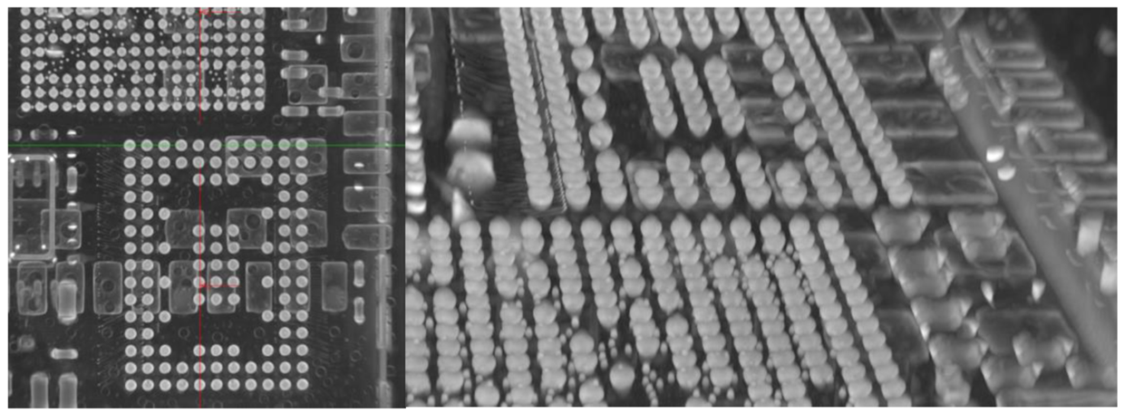
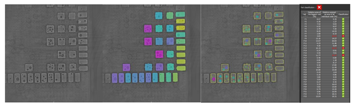
Launched in 2019, the VoidInspect workflow project between ORS and IXS had a tangible customer problem to solve from the start: Enabling the rapid non-destructive analysis of voids (enclosed cavities) inside the solder joints of board components, especially for ball grid arrays, to ensure the proper thermal stability.
The choice of laminography, as opposed to conventional computed tomography (CT), seemed the obvious solution to this challenge. This is because CT requires a small sample size to create a high-quality 3D model. In surface mount technology, this means destroying the printed circuit board, as the area of interest must be separated out. But computed laminography, which cuts a 3D volume into virtual slices for analysis, is non-destructive and can be performed over the entire inspection area while achieving high resolution. This technique, combined with new intelligent algorithms, reduces waste and inspection time by automatically localizing the slice with the best resolution to highlight and evaluate the problematic defects. As Peter Koch reports, “We can gain up to 80% in speed compared to conventional methods”.

In order to complete the evaluation even faster, its execution can be performed even by an untrained operator – with a minimum number of steps and no physical interaction. A goal that was clear from the beginning was that VoidInspect’s user interface needed to be user-friendly.
The rapid, high-quality results are achieved through a combination of several ingredients: the Yxlon image processing (the best on the market), the workflow itself, the high-end hardware, and the FF CT software ensuring quality in the reconstruction of the laminography data. It all adds up to a perfect recipe for precision. Even now, the VoidInspect workflow can be added to any FF CT software from Yxlon for off-line applications.

“The requirements we received from the team in Hamburg were extremely precise. We knew from day one what was expected and where we were headed.“
Mathieu Gendron
Lead Architect for VoidInspect, Object Research Systems (ORS), Montreal, Canada